A simple process for producing 2D materials

Ever since the discovery of the two-dimensional form of graphite (graphene) almost 20 years ago, interest in 2D materials with their special physical properties has skyrocketed. An international team of surface scientists has now developed a simple method, dubbed kinetic in situ single-layer synthesis (KISS), to produce large and very clean 2D samples from a range of materials using three different substrates.
2D materials have physical properties that are not shared by bulk material; the confinement of charge carriers is one reason for this. There are two ways to produce these 2D materials: exfoliating a larger crystal or growing a 2D layer.
Exfoliation means peeling off layers from a larger crystal until you are left with just one layer; famously, graphene was produced by exfoliating bulk graphite using sticky tape. But as noted by Antonija Grubisic-Cabo from the University of Groningen, “This process is time-consuming and requires specific skills and equipment. Furthermore, it often results in very small flakes, while the adhesive tape that is used can leave polymers on their surfaces.”
Growing 2D films, meanwhile, enables the production of large samples under controlled conditions. “However,” Grubisic-Cabo noted, “it often takes a lot of time to work out how to grow such 2D materials, and the process doesn’t always result in a perfect layer.” In response to this, Grubisic-Cabo assembled a team to develop a simple technique for the production of 2D materials, which they have described in the journal Advanced Science.
“We knew of some experiments in which gold films were used to exfoliate bulk material,” Grubisic-Cabo said. “But these were mainly performed in air, which means that this technique is not very suitable for air-sensitive materials, or for surface science research.”
The team wanted a technique that would allow production of air-sensitive 2D materials on a range of substrates. In their first attempt, they used a gold crystal in a high vacuum chamber.
“We basically slammed the crystal on bulk material and discovered that a nice 2D layer stuck to the gold,” Grubisic-Cabo said. Why this happens is not yet clear, but the team suspects that the bond with the gold is stronger than the Van der Waals force that keeps the layers in the bulk crystal together.
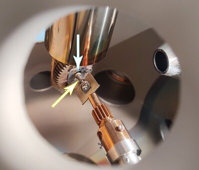
They have now built on this first experiment, adding a spring to the stage with the bulk material which acts as a shock absorber and thus allows better control of the impact of the gold crystal. Furthermore, the team showed that both silver and the semiconductor germanium could be used as a substrate to peel off 2D materials.
“Gold crystals are a standard feature in surface science labs, where they are used in the calibration of instruments, for example. Scientists don’t like to damage these crystals, but that didn’t happen in these experiments,” Grubisic-Cabo said. “And we have since changed the protocol to use single crystal gold thin films. This has the added advantage of being able to dissolve the gold so that we can isolate the 2D sample, as long as it is stable in air or liquid.”
These isolated samples may be used for the next stage: building devices from the 2D materials that will be produced using the new technique.
“This is not yet possible, but we are working on it,” Grubisic-Cabo said. “So, what we do have is a technique to produce very clean, large 2D samples in a very simple way, which allows us to create air-sensitive 2D materials. Furthermore, our technique uses standard equipment that is present in virtually every surface science laboratory.”
Microplastics found to alter the human gut microbiome
Microplastic-treated cultures showed a consistent and significant increase in acidity (lower pH...
Sustainable, self-repairing, antimicrobial polymers developed
From medicine to electronics and optics, new materials developed by scientists at Kaunas...
A better way to create conductive polymers
New research disproves the longstanding belief that to create conductive polymers, substances...


